TECHNOLOGY
Laser Diodes Built on World Class Technology
Our Discrete Mode (DM) laser platform is at the core of our products. It allows us to drive the adoption of laser technology in new industries and markets. Our proprietary manufacturing technology allows us to produce custom laser designs at any wavelength in the NIR – MIR with performance equivalent to or better than other DFB platforms.

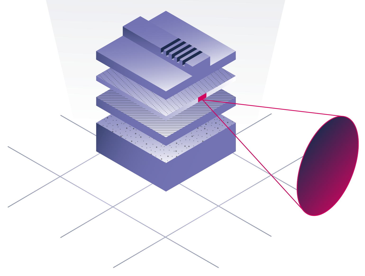
THE DISCRETE MODE LASER DIODE
Invisible
RIDGE WAVEGUIDE PROCESS
Eblana utilize a standard Fabry-Perot ridge waveguide process to fabricate the base laser structure, ensuring high reliability and consistency.
DISCRETE MODE PROCESS
Wavelength selective features are etched using surface level lithography in order to create single mode lasers. This process is highly accurate and customisable.
MQW STRUCTURE
Multiple quantum-well epitaxial structure is grown by MOCVD or MBE.
MATERIAL SYSTEM
Compared with traditional DFB approaches, our Discrete Mode technology is regrowth free and the wavelength selection material agnostic.

OUR INNOVATION PROCESS
The team at Eblana Photonics is vastly experienced in all areas of laser manufacture, from epitaxial structure design, to III-V processing and etch chemistry, all the way to backend test, coating and packaging.
Eblana Photonics lasers are designed from the ground up to suit a multitude of applications and customers. Our team has the ability to create custom laser diode designs to customer specifications, focusing on a number of key areas:
Invisible
DESIGN
Designing and growing suitable multiple quantum-well epitaxial material, with a focus on low loss and accurate PL.
SELECTIVITY
Application of the patented Discrete-Mode process to create laser diodes with custom wavelength specifications, or other optoelectronic devices such as superluminescent diodes and integrated lasers.
PACKAGING
Designing and testing advanced photonics packaging solutions for both custom and high-volume requirements.
OUR KEY ADVANTAGES
VOLUME CAPABLE
Eblana Photonics patented Discrete-Mode platform is suitable for high volume manufacturing with a focus on consistency, yield and performance.
SCALABLE
Eblana leverages well-established telecoms supply chains to ensure full scalability from sample volumes of custom wavelengths up to high volume telecom and gas sensing OEM requirements, culminating in the launch of a new backend facility in Taiwan for mass market chip and bar testing, pick and place, cleave and die bonding.
COST DISRUPTIVE
Eblana Photonics commitment to cost-disruptive packaging solutions results in a product that is driving down the cost of integrating laser diodes into sensing products.
CONTACT US
Talk to us right now to find out how Eblana Photonics can drive value for you or your team in the field.
